.png)
_upscayl_1x_upscayl-standard-4x.png)
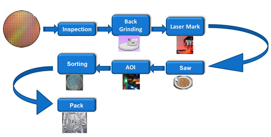
Product assembly flow
SFM8801 ---WLCSP assembly and TnR Packing
SFM8801 is packaged with WLCSP type, which includes bumping + backend packaging process. It has following advantages:
1. Miniaturization and Light Weighting
Ø Size Minimization - The size of the WLCSP package is almost equal to the original size of the bare chip. There are no additional structures such as lead frames, plastic packages, or substrates, achieving "package size ≈ chip size". This is the physical size limit that can be achieved with all current packaging technologies.
Ø Thinness maximization - The package is extremely thin, usually only a little thicker than the chip itself (mainly due to the height of the bumps/solder balls). This is a crucial advantage for ultra-thin mobile devices that are extremely sensitive to space, such as smartphones, true wireless headphones, ultra-thin laptops, and wearable devices.
2. Outstanding Electrical Performance
Ø Ultra-short interconnect path---signals directly combine from the transistors on the chip through the redistribution layer on the wafer surface to the solder balls, and then directly reach the PCB board. This completely eliminates the parasitic inductance, capacitance and resistance brought by the bonding wires, lead frames or packaging substrates in traditional packaging.
Ø Low signal delay and noise: The shortest interconnect path means faster signal transmission speed and lower delay. Fewer parasitic effects result in lower signal attenuation and power noise.
Ø Excellent heat dissipation performance: The backside of the chip (the silicon itself) can be exposed directly, or coated with a heat-conductive material and directly contact the heat sink/enclosure. Heat can be dissipated from the heat source (the chip) to the outside through the shortest path, with extremely low thermal resistance and high heat dissipation efficiency.
SFM8801 bumping and backend process flow as below:
Wafer Bumping Process Flow
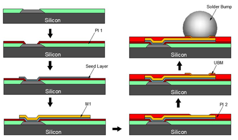
WLCSP Backend assembly process flow
SFM8801 Packing---Tape and Reel (TnR)
SFM8801 is shipped in standard TnR tape packaging, using industry-standard 8mm wide carrier tape. Each reel contains 10,000 units of the product. TnR tape packaging arranges the loose-packed and small electronic components in an orderly manner at fixed intervals and directions, sealing them within a long carrier tape, and then rolling it into a reel. It is not only a carrier for transportation and storage but also a key bridge in modern electronic manufacturing connecting component suppliers with surface mount production lines. It has the following advantages:
Ø Dust and moisture protection---the tape (usually heat-sealed or pressure-sensitive) seals the components within the tape cavity, effectively isolating dust, moisture, and impurities in the air, especially crucial for sensitive components (such as ICs, chips).
Ø Electrostatic discharge (ESD) protection---for electrostatic-sensitive devices, tape with ESD-resistant materials (such as black ESD tape ) can be used for packaging to prevent damage to the components during transportation and storage due to static electricity.
Ø Vibration and scratch protection---each component has its own position, avoiding collisions, friction, and scratches between components, especially for devices with precise pins or sensitive surfaces.
Ø Lid protection and scattering prevention---sealed packaging ensures that components do not spill during handling, maintaining order and integrity.
SFM8801 TnR packing pin1 direction instruction

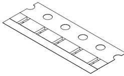
Direction of carrier tape movementààà Pin1 Direction
.png "图片7(1).png")
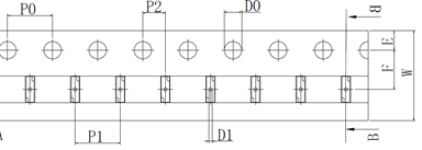
Item | W/mm | E/mm | F/mm | D0/mm | D1/mm | P0/mm | P1/mm | P2/mm |
Value | 8.0 | 1.75 | 3.5 | 1.55 | 0.3 | 4.0 | 4.0 | 2.0 |